
Fraunhofer IPMS and DiveSemiconductor Processes optimized
Together with Dive imaging systems, the Fraunhofer Institute for Photonic Microsystems IPMS has established a step towards resource-saving semiconductor production. The installation of an optical measuring device from Dive in the Fraunhofer IPMS clean room has significantly reduced the amount of inspection work required during wafer production.
Page [1 of 1]
 | | | Image 1 of 1 | | | |
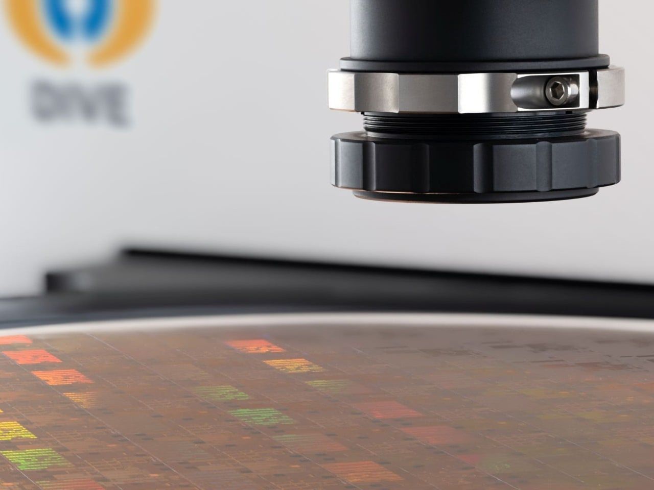
Imaging systems from DIVE enable non-destructive wafer inspection © Dive imaging system