
Image processing
CCD versus CMOS
CMOS sensors are replacing CCD sensors in many places. However, this does not mean that CCD sensors have had their day - both technologies have specific advantages and disadvantages. Which sensor is suitable for which application scenarios?
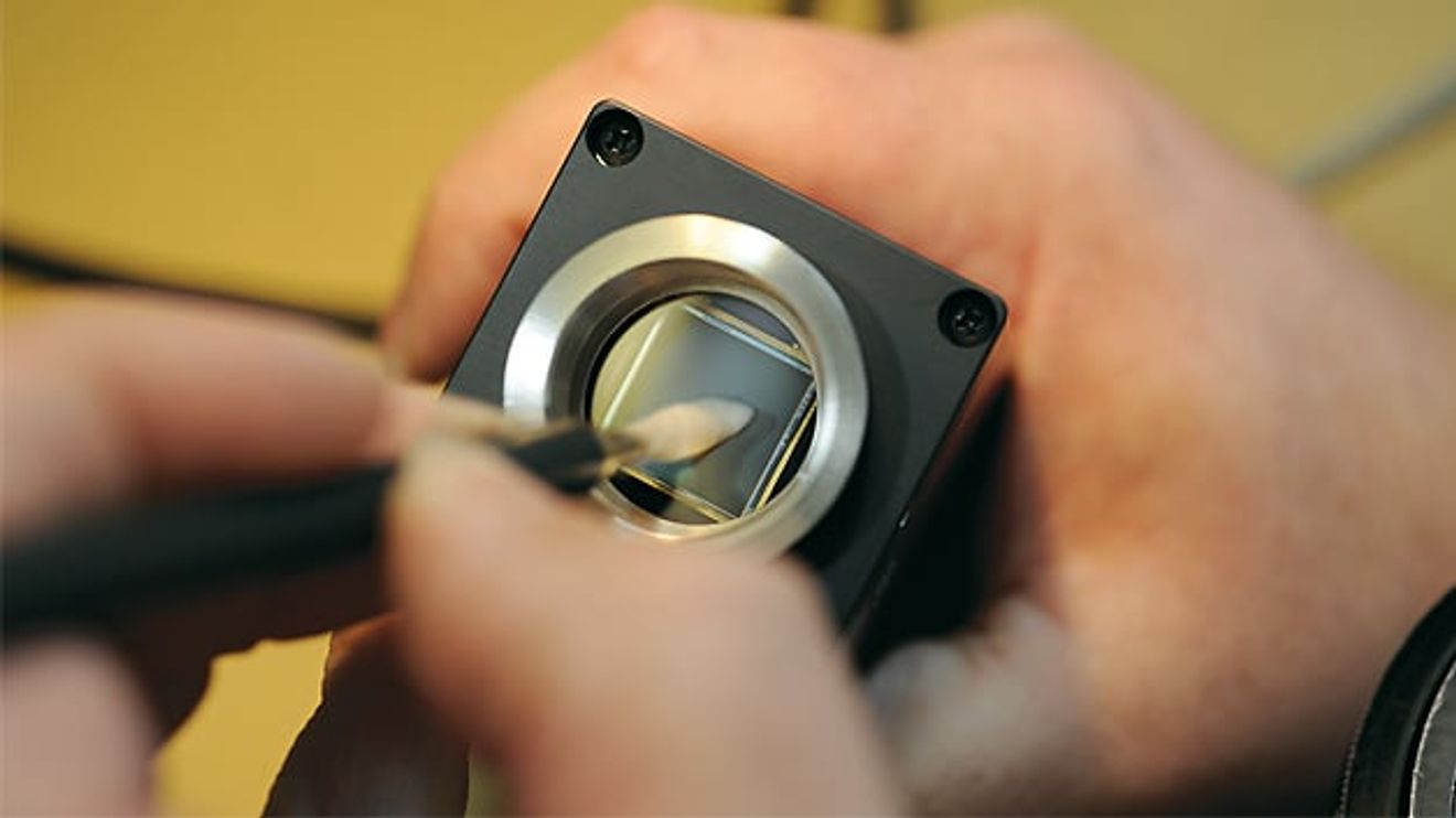
When Sony announced the discontinuation of its CCD sensors for 2026, this information raised many questions. After all, users in the field of industrial image processing have appreciated CCD sensors for many years - primarily because of their high image quality and good global shutter functionality. The fact that Sony, as one of the leading sensor manufacturers, is focusing on CMOS sensor technology could indicate that this technology has now been developed to such an extent that the majority of applications can be operated with CMOS sensors. But can CCD sensors generally be replaced by CMOS sensors in the future without any restrictions?
Silicon quantum detectors
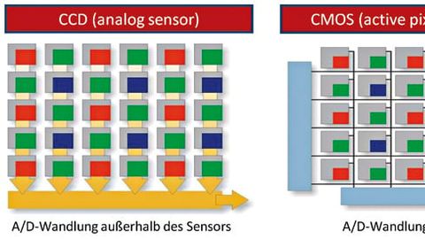
CCD and CMOS sensors are quantum detectors. Both technologies are based on the semiconductor material silicon and are therefore sensitive in the same spectral range from approx. 300 to 1000 nm. They differ primarily in the point at which the charge is converted into voltage on the semiconductor element: On a CCD sensor, vertical and horizontal charge transport takes place first. The serial charge/voltage conversion of all pixels takes place outside the sensor in the camera electronics. All pixel charges are converted into an analog voltage via an output outside the sensor.
With CMOS sensors, on the other hand, the charge/voltage conversion takes place in each pixel of the sensor. Depending on the activated line, the signal is amplified, noise-minimized and digitized via the readout circuit and finally transmitted in parallel via a configurable number of LVDS lines (Low Voltage Differential Signaling). This results in significant differences in image quality, resolution and refresh rate.
Old iron CCD sensors?
In a CCD sensor, all pixel charges are converted into an analogue voltage via an output, amplified and digitized. This results in high pixel homogeneity, a very uniform signal with low spatial noise (fixed pattern noise) and typically low dark current and therefore high image quality.
In addition, CCDs achieve high sensitivity and good signal quality at low light intensities due to the higher fill factor (ratio of the photosensitive area to the total pixel area).
Another advantage is the perfect global shutter, i.e. the simultaneous exposure of all pixels. For this reason, CCDs are very well suited for machine vision applications, particularly for applications that require very short exposure times.
However, one disadvantage of CCD sensors is the limited readout speed of the serial data stream. Modern CCDs with higher resolutions are therefore often manufactured using multi-tap technologies (division of the sensor into several image areas) in order to achieve n times the readout speed of single-tap sensors. However, a signal adjustment of the taps is then necessary, as even very small deviations lead to visible differences at the limits of the taps.
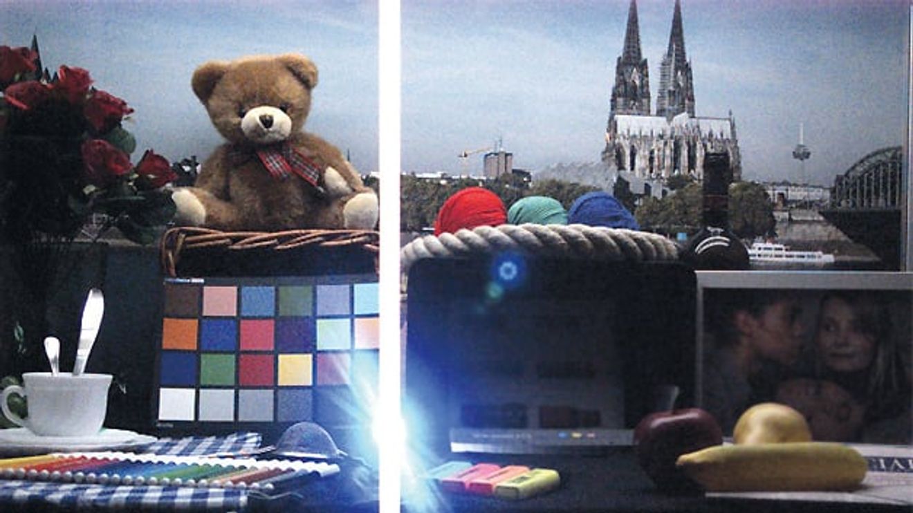
Another shortcoming of CCD sensors is that charges greater than the full-well capacity of the pixel cell reach neighboring pixels. This is visible in the typical blooming effects. This can only be remedied by reducing the amount of incident light. In addition, during readout, incident photons can generate additional charge carriers during serial charge transport in the vertical shift register - this is known as smearing. This smearing can be prevented by using a mechanical shutter in front of the sensor or by using flash illumination.
With a CMOS sensor, the charge/voltage conversion takes place at each pixel and the image information is already converted into digital information on the CMOS sensor chip. This mode of operation requires increased design complexity. CMOS designs with global shutter and CDS (correlated double sampling to reduce spatial noise) are based on pixel cells with five to eight transistors and thus reduce the light-sensitive area per pixel. Each column or pixel has an amplifier that works independently of the others. Due to technological deviations, there is a lack of uniformity between the pixels of the individual columns, which in turn leads to increased spatial noise.
Objects in motion
For applications with moving objects, a global shutter function is required for the sensors. This requires a memory area on the pixel in the CMOS sensor that is as well shielded from light as possible. In practice, this is not the case, especially with older CMOS designs - the area is more or less sensitive to light and shows a parasitic light sensitivity during the readout of the pixel data. Especially with short exposure times in the microsecond range, this is clearly visible as a vertical gray value gradient.
However, the parallel readout of image information from a CMOS sensor offers the advantage of higher frame rates at comparable resolutions, depending on the number of LVDS lines. Furthermore, it is possible to achieve faster and more flexible readout by directly addressing individual pixels via one or more image areas (region of interest). As the charges do not have to be shifted vertically and horizontally in the CMOS sensor, but are converted into a voltage directly at the pixel, the blooming and smearing artifacts do not occur. CMOS sensors can therefore handle high light intensities. Using high dynamic range mode within an image capture, it is possible to visualize high-contrast, extremely bright objects as well as darker image areas, resulting in images with a high dynamic range.

Another advantage of CMOS sensor technology is the integration of the control circuit (clock generation, amplifier, A/D converter) on the sensor chip. The construction of a camera is therefore more cost-effective and has a lower power consumption compared to CCDs.
CMOS sensors are therefore the first choice for machine vision applications that require high frame rates in conjunction with high resolution. One example is a laser triangulation application for 3D measurements, in which a camera with a high-speed CMOS sensor with a resolution of 2320 x 128 pixels scans 5200 profiles per second. For this type of application, in addition to a high frame rate, it is crucial that CMOS sensors can handle high light intensities well, especially for materials with reflective surfaces.
The challenge of light
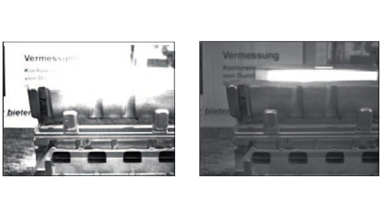
Capturing single images of scenes with extreme light contrasts requires sensors with special exposure control. With the CMV300 CMOS sensor, the degree of saturation of the pixels is ...
© Allied Vision TechnologiesCMOS technology has also made significant progress in image quality in recent years. Modern CMOS sensors with global shutter are available in different resolutions and with high frame rates, for example sensors with more than 500 fps at VGA resolution. By reducing dark and spatial noise and increasing quantum efficiency, the sensors deliver good image quality even at low light intensities.
The parasitic light sensitivity of the memory during readout has also been significantly reduced - resulting in improved global shutter efficiency with values in the range of 10,000:1 or better. This means that modern CMOS sensors are also suitable for applications with moving objects. Assuming a readout time of 10 ms (at 100 fps), for example, the parasitic light sensitivity would be just 1 µs, which is not critical for most applications with moving objects.
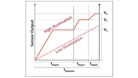
... in HDR mode (High Dynamic Range Image) specifically controlled via 'knee points'.
© Allied Vision TechnologiesSony's CMOS pixel architecture Pregius is exemplary. An analog memory shielded from light ensures a perfect global shutter. A double CDS stage and other technological optimizations of the pixel design minimize the readout noise to single-digit values. This enables images with shorter exposure times and consequently less motion blur of fast-moving objects.
This makes modern CMOS sensors suitable for industrial image processing applications as well as for outdoor applications with high light contrasts, such as in the field of security and intelligent transportation systems.
Refugia for CCD sensors
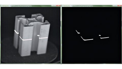
Laser triangulation for 3D measurements of profile strands: In addition to the high frame rate of 5200 frames/s, this application requires tolerance to high light intensities.
© Allied Vision TechnologiesDue to the very homogeneous image quality with low spatial noise, CCD sensors have advantages for medical and scientific applications, especially for fluorescence microscopy and high-resolution microscopy. CCD sensors are also suitable for applications such as aerial mapping, which require a very high resolution. Due to the minimal dark current, the sensors also offer advantages for applications with long exposure times, for example for applications in astronomy.
Manufacturers such as OnSemi, Sharp or e2v will continue to develop CCD technology in the future and offer special CCD sensors with higher resolution (e.g. 50 MP) and higher sensitivity for demanding applications in the scientific field, particularly for metrology applications where high image homogeneity at high resolution is required.
Special CCD sensors such as EMCCDs (Electron Multiplication CCD) with a very high dynamic range are optimized for imaging in day and night light, for applications with extremely low light levels or applications such as molecular and cell investigations. Improvements in CCD design include optimized microlens arrangements, special epitaxial doping and increased substrate thickness for improved sensitivity in the visible and NIR range.
Author:
Jürgen Bretschneider is Head of Content Management at Allied Vision Technologies in Stadtroda.


You might also be interested in
2D Machine Vision brands bundled under one roof
From January 2026, the image processing brands Allied Vision, Chromasens, Mikrotron, NET and SVS-Vistek will be merged under the Allied Vision brand. The companies, which are part of TKH Group NV, will combine their technological know-how,...
 read more...
Robert Franz is the new CEO
SVS-Vistek founder and CEO Walter Denk has retired from operational business at the end of 2023. Robert Franz took over as CEO on January 1.
read more...SWIR hyperspectral camera for industrial high-speed inspection
Teledyne Dalsa launches 'Kaleido', a hyperspectral camera for use in the shortwave infrared (SWIR) range, designed to overcome the existing integration and performance limitations of industrial sorting processes.
read more...Machine vision industry expects turnaround in 2026
After difficult years, the European machine vision industry is sending out the first signs of recovery: growth is expected again in 2026 - driven by global demand, AI and automation. However, uncertainties and weak investment in Europe continue to...
read more...Basler and Orbbec launch Technology Partnership
Basler, a provider of machine vision components and solutions, and Orbbec, a specialist in 3D vision technology and robotics, have announced a strategic partnership to implement industrial 3D solutions for factory and logistics automation.
read more...For critical tasks in logistics automation
The Cognex 'Solutions Experience (SLX)' product range comprises application-specific solutions for critical automation tasks in key industrial sectors.
read more...IDS and Prophesee intensify partnership
IDS and Prophesee are intensifying their partnership for the next generation of event-based industrial cameras. Together they want to explore new sensor architectures that combine classic imaging with Prophesee's event-based 'Metavision' technology.
read more...Dynamic OCR Inspection
Due to strict compliance regulations, packaging containing medical products must be correctly labeled before it is delivered to customers. The Chinese company Shenzhen Jiangrun Xuneng Technology has developed a sophisticated image processing...
read more...Camera for simplified AI-based Quality Controls
Omron's 'FHV7-AI' detection camera joins the company's family of industrial FH vision vision systems. The new model combines AI-powered inspection capabilities with a simplified user interface and a compact all-in-one design.
read more...